GaAs Wafers
GaAs Wafers
GaAs WAFER
Semiconductor materials can be subdivided into substrates, targets, chemical and mechanical polishing materials, photoresists, electronic wet chemicals, electronic specialty gases, packaging materials and so on. Among them, substrates are one of the key materials in the field of semiconductor materials. Gallium arsenide (GaAs), as a representative of the second generation semiconductor substrate materials, is the world's most widely used and most extensively produced compound semiconductor material, and one of the most important microelectronic materials following silicon (Si) materials. As GaAs has a low intrinsic carrier concentration, good photoelectric properties, high electron mobility (5-6 times that of silicon), a large forbidden band width (1.43eV, silicon is 1.1eV) and a direct bandgap,it is being widely used in RF devices and optoelectronic devices. The RF devices made of GaAs have the advantages of high frequency, good performance, low noise, and radiation resistance, and are able to meet the needs of a variety of applications.
We produce 2-inch to 6-inch GaAs wafers according to customers' needs, in LED grade, laser LD grade, and RF grade. The wafers can be processed as single-or double-sided polished, lasermarked, packaged in a single piece or a cassette, ready to use out of the box.
Application Fields
Currently, GaAs is widely used in smart phones, optical communications, satellite communications, LED displays and solar cells. GaAs substrates are categorized into semi-insulating substrates and semiconductor substrates. Semi-insulating GaAs substrates are mainly used to make RF devices. As the core component of wireless communication, RF chips consist of power amplifier, RF switch, RF filter, low-noise amplifier, etc. Semiconductor GaAs substrates are mainly used to make optoelectronic devices, including LEDs, lasers and so on. Driven by 5G communications, next-generation displays (MiniLED, MicroLED), LiDar, and wearable devices, the market size of gallium arsenide is continuing to expand. VCSEL chips were first introduced into Apple phones in 2015, and then gradually applied to the automotive field for monitoring driver status and fatigue driving. The global market size is expected to reach USD4 billion by 2027.
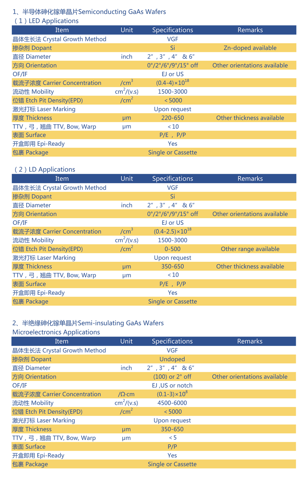
PRODUCT SPECIFICATIONS